How to achieve efficient 600W transient protection in a limited space? Analysis of Circuit Design Based on HTPSMB100 (C) A
How to Achieve Efficient 600W Transient Protection in Limited Space? Circuit Design Analysis Based on HTPSMB100(C)A
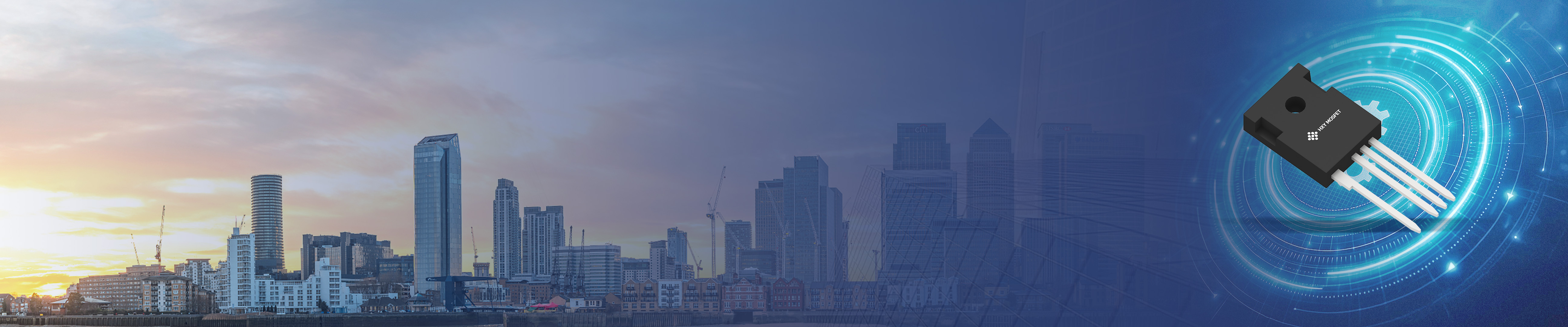
In embedded hardware design, interface protection often represents the "last mile" in determining product stability. Particularly in industrial communication and power port designs, engineers frequently face a dilemma: meeting stringent surge protection standards while being constrained by premium PCB layout space. Traditional protection solutions are often bulky or suffer severe performance degradation in high-temperature environments. Addressing this pain point, Huaxuanyang Electronics (HXY MOSFET) has introduced the HTPSMB100(C)A Transient Voltage Suppressor (TVS), offering a highly competitive domestic alternative for achieving high-reliability protection in compact designs.
Core Parameters Analysis: 600W Protection in a Compact Package
This product utilizes a compact SMB (DO-214AA) surface-mount package, highly suitable for automated production. Its core parameters directly address application pain points:
Peak Pulse Power: Under the 10/1000μs standard waveform, it features 600W peak pulse power dissipation capability. This enables effective absorption of common Electrostatic Discharge (ESD) and Electrical Fast Transient (EFT) burst interference.
Bidirectional and Unidirectional Versions: The "C" in the model number indicates Bidirectional, while the version without "C" is Unidirectional. The unidirectional version (HTPSMB100A) is typically used in DC circuits, while the bidirectional version (HTPSMB100CA) is more suitable for AC lines or bidirectional signal lines.
Key Voltage Parameters:
Stand-off Voltage (VRWM): 85.5V. This means under normal operating conditions, the device presents high impedance to circuits below 85.5V, generating no leakage current interference.
Breakdown Voltage (VBR): Minimum 95V, maximum 105V. When voltage exceeds this range, the device conducts rapidly.
Maximum Clamping Voltage (VC): 137V. This represents the maximum voltage level the device can limit under peak pulse current (4.5A). Lower clamping voltage provides better protection for downstream sensitive MCUs or communication chips.
Technical Highlights: Why Choose This Device?
Based on the technical characteristics specified in the datasheet, this device offers the following significant advantages in practical applications:
Glass Passivated Die: This process significantly enhances the device‘s environmental adaptability, improving resistance to moisture and contamination, ensuring stable operation under harsh conditions.
Low Inductance and Fast Response: The datasheet specifically mentions "Low inductance" and "Fast Response Time". For high-frequency transient interference, low inductance means reduced parasitic effects, enabling picosecond (ps) response speed to instantly discharge high voltage to ground.
Excellent Clamping Capability: Superior clamping capability means that when surges occur, it acts like a "voltage ceiling," firmly suppressing threat voltages within safe limits, protecting expensive downstream main control chips.
Typical Application Scenarios
Based on the mechanical data and application recommendations provided in the datasheet, the HTPSMB100(C)A is well-suited for the following scenarios:
AC/DC Power Adapters: Serving as secondary protection at the input stage to prevent damage to power modules from lightning-induced surges or grid fluctuations.
Low-frequency Signal Transmission Lines: Such as RS232, RS485, and other industrial bus interfaces. These interfaces are frequently exposed to external environments, making them susceptible to electrostatic or induced voltages. This device effectively protects communication interfaces from damage.
I/O Interface Protection: Any input/output ports requiring Electrostatic Discharge (ESD) protection.
Design Recommendations and Pitfall Avoidance Guide
To ensure the HTPSMB100(C)A delivers optimal performance, the following PCB layout recommendations are provided based on experienced engineers‘ expertise:
Keep Traces Short: As the TVS diode functions to rapidly divert surge current to ground, traces from the interface to the TVS, and from the TVS to the ground point, must be as short and wide as possible. Excessive trace length introduces parasitic inductance, causing additional induced voltage (V=L*di/dt) during transient events, which may subject downstream chips to spike voltages higher than the TVS clamping voltage.
Thermal Considerations: While the device‘s peak power rating is 600W, the datasheet indicates only 5W average power dissipation at TA=50°C for continuous thermal dissipation. If your application operates at high ambient temperatures or experiences extremely high surge frequencies (beyond non-repetitive pulses), ensure adequate copper foil area is reserved on the PCB as thermal pads, or consider derating the device.
Polarity Attention: If selecting the unidirectional version (HTPSMB100A), pay careful attention to the PCB silkscreen orientation; reverse installation will cause circuit short-circuit.
About Huaxuanyang Electronics
Huaxuanyang Electronics (HXY MOSFET), as a professional power device solutions expert, is committed to providing customers with full-scenario device empowerment. From R&D design to precision manufacturing, Huaxuanyang not only provides high-quality domestic components but also strives to help customers achieve supply chain autonomy through one-stop services. In the current complex market environment, selecting cost-effective domestic solutions like the HTPSMB100(C)A is an effective way to reduce BOM costs and enhance product competitiveness.
Disclaimer:
This article is written based on information provided in Huaxuanyang Electronics‘ datasheets for reference only. Parameters, application circuits, and recommendations mentioned herein do not constitute final design guarantees. In actual product design, please refer strictly to the latest official datasheet and conduct thorough prototype testing. Huaxuanyang Electronics assumes no legal liability for equipment failures resulting from the use of information in this article.


 Contact
 E-mail
 ChatNow